Infoportal
Inhaltsverzeichnis
Steckerbelegung
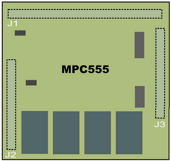
Stecker J1
| Pin | Signal | Beschreibung |
|---|---|---|
| 1 | +3.3V | 3.3 V Versorgung |
| 2 | GND | Masse |
| 3 | A:TPU0 | TPU-A: Kanal 0 |
| 4 | A:TPU1 | TPU-A: Kanal 1 |
| 5 | A:TPU2 | TPU-A: Kanal 2 |
| 6 | A:TPU3 | TPU-A: Kanal 3 |
| 7 | A:TPU4 | TPU-A: Kanal 4 |
| 8 | A:TPU5 | TPU-A: Kanal 5 |
| 9 | A:TPU6 | TPU-A: Kanal 6 |
| 10 | A:TPU7 | TPU-A: Kanal 7 |
| 11 | A:TPU8 | TPU-A: Kanal 8 |
| 12 | A:TPU9 | TPU-A: Kanal 9 |
| 13 | A:TPU10 | TPU-A: Kanal 10 |
| 14 | A:TPU11 | TPU-A: Kanal 11 |
| 15 | A:TPU12 | TPU-A: Kanal 12 |
| 16 | A:TPU13 | TPU-A: Kanal 13 |
| 17 | A:TPU14 | TPU-A: Kanal 14 |
| 18 | A:TPU15 | TPU-A: Kanal 15 |
| 19 | A:TPUCLK | TPU-A: Taktsignal |
| 20 | A:AN0 | ADC-A: Kanal 0 |
| 21 | A:AN1 | ADC-A: Kanal 1 |
| 22 | A:AN2 | ADC-A: Kanal 2 |
| 23 | A:AN3 | ADC-A: Kanal 3 |
| 24 | A:AN48 | ADC-A: Kanal 48 |
| 25 | A:AN49 | ADC-A: Kanal 49 |
| 26 | A:AN50 | ADC-A: Kanal 50 |
| 27 | A:AN51 | ADC-A: Kanal 51 |
| 28 | A:AN52 | ADC-A: Kanal 52 |
| 29 | A:AN53 | ADC-A: Kanal 53 |
| 30 | A:AN54 | ADC-A: Kanal 54 |
| 31 | A:AN55 | ADC-A: Kanal 55 |
| 32 | A:AN56 | ADC-A: Kanal 56 |
| 33 | A:AN57 | ADC-A: Kanal 57 |
| 34 | A:AN58 | ADC-A: Kanal 58 |
| 35 | A:AN59 | ADC-A: Kanal 59 |
| 36 | ETRIG1 | Trig für ADC-A |
| 37 | B:AN0 | ADC-B: Kanal 0 |
| 38 | B:AN1 | ADC-B: Kanal 1 |
| 39 | B:AN2 | ADC-B: Kanal 2 |
| 40 | B:AN3 | ADC-B: Kanal 3 |
| 41 | B:AN48 | ADC-B: Kanal 48 |
| 42 | B:AN49 | ADC-B: Kanal 49 |
| 43 | B:AN50 | ADC-B: Kanal 50 |
| 44 | B:AN51 | ADC-B: Kanal 51 |
| 45 | B:AN52 | ADC-B: Kanal 52 |
| 46 | B:AN53 | ADC-B: Kanal 53 |
| 47 | B:AN54 | ADC-B: Kanal 54 |
| 48 | B:AN55 | ADC-B: Kanal 55 |
| 49 | B:AN56 | ADC-B: Kanal 56 |
| 50 | B:AN57 | ADC-B: Kanal 57 |
| 51 | B:AN58 | ADC-B: Kanal 58 |
| 52 | B:AN59 | ADC-B: Kanal 59 |
| 53 | ETRIG2 | Trigger für ADC-B |
| 54 | NC | Nicht verbunden |
| 55 | NC | Nicht verbunden |
| 56 | MDA31 | Double Action Modul Pin 31 |
| 57 | MDA30 | Double Action Modul Pin 30 |
| 58 | MDA29 | Double Action Modul Pin 29 |
| 59 | MDA28 | Double Action Modul Pin 28 |
| 60 | MDA27 | Double Action Modul Pin 27 |
| 61 | MDA15 | Double Action Modul Pin 15 |
| 62 | MDA14 | Double Action Modul Pin 14 |
| 63 | MDA13 | Double Action Modul Pin 13 |
| 64 | MDA12 | Double Action Modul Pin 12 |
| 65 | MDA11 | Double Action Modul Pin 11 |
| 66 | MPWM0 | Multiple PWM Module Pin 0 |
| 67 | MPWM1 | Multiple PWM Module Pin 1 |
| 68 | MPWM2 | Multiple PWM Module Pin 2 |
| 69 | MPWM3 | Multiple PWM Module Pin 3 |
| 70 | MPWM6 | Multiple PWM Module Pin 6 |
| 71 | MPWM7 | Multiple PWM Module Pin 7 |
| 72 | MPWM8 | Multiple PWM Module Pin 8 |
| 73 | MPWM9 | Multiple PWM Module Pin 9 |
| 74 | MPIOB4/VFLS1 | Digitale I/O, Kanal 4 |
| 75 | MPIOB3/VFLS0 | Digitale I/O, Kanal 3 |
| 76 | MPIOB2/VF2 | Digitale I/O, Kanal 2 |
| 77 | MPIOB1/VF1 | Digitale I/O, Kanal 1 |
| 78 | MPIOB0/VF0 | Digitale I/O, Kanal 0 |
| 79 | MPIOB5 | Digitale I/O, Kanal 5 |
| 80 | MPIOB6 | Digitale I/O, Kanal 6 |
| 81 | MPIOB7 | Digitale I/O, Kanal 7 |
| 82 | MPIOB8 | Digitale I/O, Kanal 8 |
| 83 | MPIOB9 | Digitale I/O, Kanal 9 |
| 84 | MPIOB10 | Digitale I/O, Kanal 10 |
| 85 | MPIOB11 | Digitale I/O, Kanal 11 |
| 86 | MPIOB12 | Digitale I/O, Kanal 12 |
| 87 | MPIOB14 | Digitale I/O, Kanal 14 |
| 88 | MPIOB13 | Digitale I/O, Kanal 13 |
| 89 | MPIOB15 | Digitale I/O, Kanal 15 |
| 90 | ECK | External Baud Clock |
| 91 | SCK | SPI Taktsignal |
| 92 | MOSI | SPI, Master out, Slave in |
| 93 | MISO | SPI, Master in, Slave out |
| 94 | PCS3 | SPI, Programmierbares Chip select 3 |
| 95 | PCS2 | SPI, Programmierbares Chip select 2 |
| 96 | PCS1 | SPI, Programmierbares Chip select 1 |
| 97 | PCS0 | SPI, Programmierbares Chip select 0 |
| 98 | EPEE | Program-Enable für internes Flash |
| 99 | GND | Masse |
| 100 | +3.3V | 3.3 V Versorgung |
Stecker J2
| Pin | Signal | Beschreibung |
|---|---|---|
| 1 | +3.3V | 3.3 V Versorgung |
| 2 | GND | Masse |
| 3 | D0 | Systembus, Datenleitung 0 |
| 4 | D1 | Systembus, Datenleitung 1 |
| 5 | D2 | Systembus, Datenleitung 2 |
| 6 | D3 | Systembus, Datenleitung 3 |
| 7 | D4 | Systembus, Datenleitung 4 |
| 8 | D5 | Systembus, Datenleitung 5 |
| 9 | D6 | Systembus, Datenleitung 6 |
| 10 | D7 | Systembus, Datenleitung 7 |
| 11 | D8 | Systembus, Datenleitung 8 |
| 12 | D9 | Systembus, Datenleitung 9 |
| 13 | D10 | Systembus, Datenleitung 10 |
| 14 | D11 | Systembus, Datenleitung 11 |
| 15 | D12 | Systembus, Datenleitung 12 |
| 16 | D13 | Systembus, Datenleitung 13 |
| 17 | D14 | Systembus, Datenleitung 14 |
| 18 | D15 | Systembus, Datenleitung 15 |
| 19 | D16 | Systembus, Datenleitung 16 |
| 20 | D17 | Systembus, Datenleitung 17 |
| 21 | D18 | Systembus, Datenleitung 18 |
| 22 | D19 | Systembus, Datenleitung 19 |
| 23 | D20 | Systembus, Datenleitung 20 |
| 24 | D21 | Systembus, Datenleitung 21 |
| 25 | D22 | Systembus, Datenleitung 22 |
| 26 | D23 | Systembus, Datenleitung 23 |
| 27 | D24 | Systembus, Datenleitung 24 |
| 28 | D25 | Systembus, Datenleitung 25 |
| 29 | D26 | Systembus, Datenleitung 26 |
| 30 | D27 | Systembus, Datenleitung 27 |
| 31 | D28 | Systembus, Datenleitung 28 |
| 32 | D29 | Systembus, Datenleitung 29 |
| 33 | D30 | Systembus, Datenleitung 30 |
| 34 | D31 | Systembus, Datenleitung 31 |
| 35 | A31 | Systembus, Adressleitung 31 |
| 36 | A30 | Systembus, Adressleitung 30 |
| 37 | A29 | Systembus, Adressleitung 29 |
| 38 | A28 | Systembus, Adressleitung 28 |
| 39 | A27 | Systembus, Adressleitung 27 |
| 40 | A26 | Systembus, Adressleitung 26 |
| 41 | A25 | Systembus, Adressleitung 25 |
| 42 | A24 | Systembus, Adressleitung 24 |
| 43 | A23 | Systembus, Adressleitung 23 |
| 44 | A22 | Systembus, Adressleitung 22 |
| 45 | A21 | Systembus, Adressleitung 21 |
| 46 | A20 | Systembus, Adressleitung 20 |
| 47 | A19 | Systembus, Adressleitung 19 |
| 48 | A18 | Systembus, Adressleitung 18 |
| 49 | A17 | Systembus, Adressleitung 17 |
| 50 | A16 | Systembus, Adressleitung 16 |
| 51 | A15 | Systembus, Adressleitung 15 |
| 52 | A14 | Systembus, Adressleitung 14 |
| 53 | A13 | Systembus, Adressleitung 13 |
| 54 | A12 | Systembus, Adressleitung 12 |
| 55 | A11 | Systembus, Adressleitung 11 |
| 56 | A10 | Systembus, Adressleitung 10 |
| 57 | A9 | Systembus, Adressleitung 9 |
| 58 | A8 | Systembus, Adressleitung 8 |
| 59 | +3.3V | 3.3 V Versorgung |
| 60 | GND | Masse |
Stecker J3
| Pin | Signal | Beschreibung |
|---|---|---|
| 1 | +5V | 5.0 V Versorgung |
| 2 | AGND | Analog Masse |
| 3 | +12V | 12 V Versorgung für CAN-Bus (optional) |
| 4 | GND | Masse |
| 5 | +3.3V | 3.3 V Versorgung |
| 6 | NC | Nicht verbunden |
| 7 | B:TPUCLK | TPU-B: Taktsignal |
| 8 | B:TPU15 | TPU-B: Kanal 15 |
| 9 | B:TPU14 | TPU-B: Kanal 14 |
| 10 | B:TPU13 | TPU-B: Kanal 13 |
| 11 | B:TPU12 | TPU-B: Kanal 12 |
| 12 | B:TPU11 | TPU-B: Kanal 11 |
| 13 | B:TPU10 | TPU-B: Kanal 10 |
| 14 | B:TPU9 | TPU-B: Kanal 9 |
| 15 | B:TPU8 | TPU-B: Kanal 8 |
| 16 | B:TPU7 | TPU-B: Kanal 7 |
| 17 | B:TPU6 | TPU-B: Kanal 6 |
| 18 | B:TPU5 | TPU-B: Kanal 5 |
| 19 | B:TPU4 | TPU-B: Kanal 4 |
| 20 | B:TPU3 | TPU-B: Kanal 3 |
| 21 | B:TPU2 | TPU-B: Kanal 2 |
| 22 | B:TPU1 | TPU-B: Kanal 1 |
| 23 | B:TPU0 | TPU-B: Kanal 0 |
| 24 | NC | Nicht verbunden |
| 25 | HardReset! | Hardware Reset |
| 26 | ClkOut | Systemtakt |
| 27 | EngClk | Engineering Clock |
| 28 | B:TX | CAN, Senden |
| 29 | B:RX | CAN, Empfangen |
| 30 | IRQ7 | Interrupt Eingang 7 |
| 31 | IRQ6 | Interrupt Eingang 6 |
| 32 | IRQ5 | Interrupt Eingang 5 |
| 33 | IRQ4 | Interrupt Eingang 4 |
| 34 | IRQ3 | Interrupt Eingang 3 |
| 35 | IRQ2 | Interrupt Eingang 2 |
| 36 | IRQ1 | Interrupt Eingang 1 |
| 37 | IRQ0 | Interrupt Eingang 0 |
| 38 | IRQOUT | Interrupt request acknowledge |
| 39 | CS3 | Chip Select Signal 3 |
| 40 | CS2 | Chip Select Signal 2 |
| 41 | NC | Nicht verbunden |
| 42 | NC | Nicht verbunden |
| 43 | NC | Nicht verbunden |
| 44 | RXD2 | SCI2, Daten empfangen |
| 45 | RXD1 | SCI1, Daten empfangen |
| 46 | TXD2 | SCI2, Daten senden |
| 47 | TXD1 | SCI1, Daten senden |
| 48 | NC | Nicht verbunden |
| 49 | BI/STS | Burst Inhibit |
| 50 | OE | Output Enable |
| 51 | TEA | Transfer Error Acknowledge |
| 52 | TA | Transfer Acknowledge |
| 53 | TS | Tansfer Start |
| 54 | BDIP | Transfer in Progress |
| 55 | Burst | Burst Indication |
| 56 | RD/WR | Read/Write |
| 57 | TSIZ1 | Transfer Size 1 |
| 58 | TSIZ0 | Transfer Size 0 |
| 59 | GND | Masse |
| 60 | +3.3V | 3.3 V Versorgung |